

Can't visualize what are Adders in Digital Logic? Here's the brief!
-Half Adder Circuit and Full Adder Circuit


🟢Introduction
🔹Adders are digital circuits that perform numerical addition. Adders are an essential component of any CPU's Arithmetic Logic Unit (ALU).
🔹Binary addition is the most commonly performed task by most common adders. Aside from addition, adders are employed in a variety of digital applications such as table index calculation, address decoding, and so on.
🔹Well Here's about binary addition: Binary addition is analogous to decimal addition. Add a number's first digits, and if the total exceeds binary 2, carry '1' to the next row.
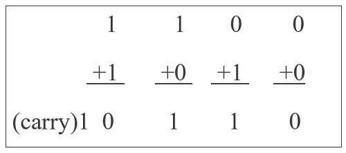
🔹Simple binary addition requires an adder with two inputs and two outputs (sum and carry). A Half Adder is the device that does the above task. Another circuit that can add three numbers is a Full Adder (two bits from the numbers and one carry bit from the previous sum).
🟢Half Adder Circuit
🔹A half adder is a combinational circuit that adds two single-bit binary values to obtain a 2-bit number. The Sum (typically denoted as Sum) is the LSB of the result, and the Carry is the MSB (usually represented as carry).

🔹Here, ‘A’ and ‘B’ represents the input two bits that must be added and the outputs are ‘Sum’ and ‘Carry’.
🔶Half Adder Truth Table
🔹Assuming A and B are the two bits to be added, a truth table for a half adder with A, B as inputs and Sum, Carry as outputs can be tabulated as follows.
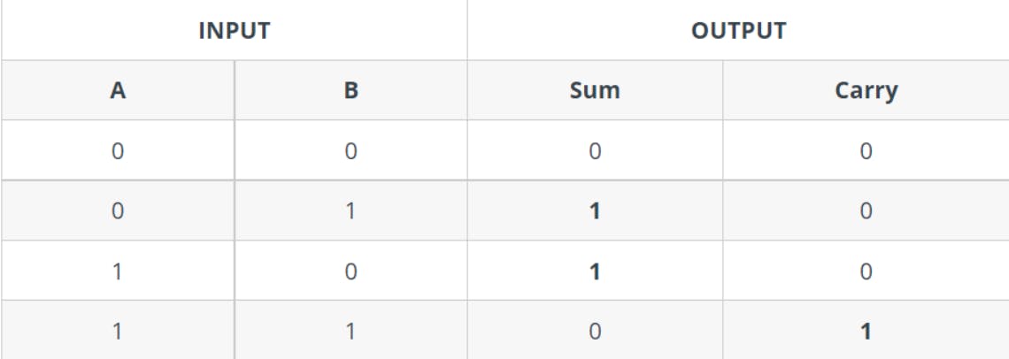
🔹According to the truth table, the total output of the binary addition performed above is similar to an Ex-OR operation, and the carry output is akin to an AND operation. The Karnaugh Map can be used to confirm this.
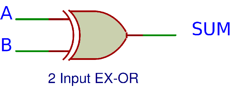
🔹We can derive the Boolean Expression of Sum as follows:
Sum = A B' + A' B
Sum = A ⊕ B
Hence, the logic diagram for the sum is shown below.
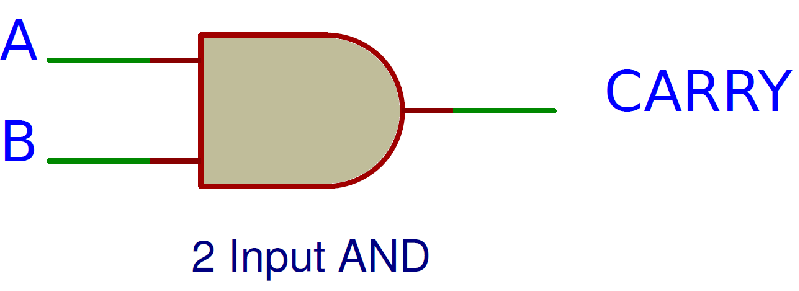
We can derive the Boolean Expression of Carry as follows:
Carry = A.B
The logic diagram for carry is shown below.
🔹NAND and NOR are known as universal gates because they can be used to create any logic system. They can also be used to implement the Half Adder Circuit. A half-adder circuit has one XOR gate and one AND gate, as we know.
🔶Half Adder using NAND Gates and XOR gates

🔹Five NAND gates are required in order to design a half-adder.
🔹Five NOR gates are required in order to design a half-adder.
🔶Limitations of Half Adder
🔹Because they cannot add the carry bit from the previous bit, these simple binary adders are referred to as Half Adders. This is a significant drawback of half adders when employed as binary adders, particularly in real-time circumstances involving the addition of several bits. Full adders are being developed to address this constraint.
🟢Full Adder Circuit
🔹A Full Adder is a Combinational Logic Circuit that performs binary addition on numbers with two digits. When compared to half adders, full adders are more sophisticated and difficult to instal.
🔹The key difference between this and a half adder is that a full adder is a digital circuit used to calculate the sum of three binary bits. Two of the three bits, A, the augend bit, and B, the addend bit, are the same as before. Carry-in refers to the additional third bit, which is a carry bit from the preceding step. It computes the sum of three bits combined with the carry. Carry-out refers to the output carry.

🔶Full Adder Truth Table
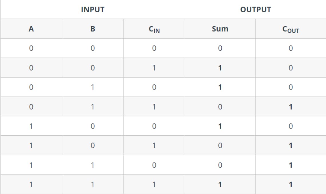
🔹Based on the truth table, the Boolean functions for Sum (S) and Carry–out (COUT) can be derived using K–Map.
🔹Using the truth table and the above K-Map, the Boolean Expression of the Sum (S) output of a Full Adder can be derived as:
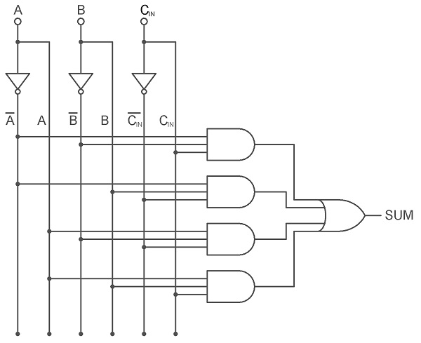
✔S = A' B' CIN + A' B C'IN + A B' C'IN + A B CIN
🔹The Sum Output of a Full Adder can be built using four 3-Input AND Gates, three NOT Gates, and one 4-Input OR Gate, according to the given Boolean Expression. The logic diagram of a Full Adder's Sum output (S) is shown in the image below.
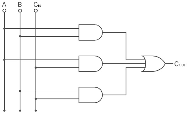
✔CARRYOUT = A B + A CIN + B CIN
🔹From the above Boolean Expression, we can say that the Carry Output of a Full Adder can be implemented using three 2-Input AND Gates and one 3-Input OR Gate. The following image shows the logic diagram of the Carry output (COUT) of a Full Adder
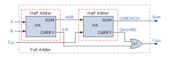
🔶Implementation of Full Adder using Half Adders
🔹By logically linking two half-adders, a complete adder can be built. The block diagram below depicts the implementation of a complete adder using two half adders.
🔶Full Adder using NAND Gates
🔹As previously stated, a NAND gate is a universal gate that may be used to build any logic design. The whole adder circuit utilising only NAND gates is shown below.
🟢Conclusion
Thank You soo Much for your time 🥳🥳. Hope you learned how to implement a Half Adder Circuit, its Boolean Equations, Logic Circuit and also design of Half Adder using NAND and NOR gates, Full Adder Circuit, its Boolean expressions, logic circuit, and implementation of Full Adder using Half Adder.
Written with heart by - MITHIN DEV
All representations belong to respective creators.